GPUs from first principles
by Janaki Ram Puli
Contents
- Computing y = a·x + y
- Memory
- Instructions and registers
- The processor
- The clock
- Long lists
- Math speed
- Memory bandwidth
- Memory latency
- How a CPU handles latency
- A chip built for throughput
- Switching between threads
- Warps
- SMs
- Blocks and shared memory
- Levels of memory
- Reusing numbers
- Overview
- Further reading
Computing y = a·x + y
Take three numbers a, x and y, multiply a by x, and add the result to y. For example, with a = 2, x = 3 and y = 4, the new y is 2·3 + 4 = 10.
A machine that does the calculation needs a place to keep the numbers, a way to write down the steps and a circuit that runs the steps.
Memory
The machine keeps its numbers in memory. Memory is a long row of storage places, and each place has a number called its address, so the machine can ask for the number at a given address.
Memory stores everything as bits, where each bit is a 0 or a 1, and 8 bits make one byte. The numbers in this note are mostly 32-bit numbers, which take 4 bytes each. If a is at address 100, then x can be at address 104 and y at address 108.
The main memory of a computer is DRAM (dynamic memory), which stores each bit as a tiny electric charge. DRAM can hold many bits in a small space, but it is made on separate chips next to the processor, so a read from it is slow.
Instructions and registers
The steps are written as instructions. Each instruction is one small step that the machine knows how to do, e.g., copy a number, multiply two numbers or add two numbers. A list of instructions is called a program.
The circuit that does the math can only work on numbers that are right next to it. The machine therefore has a few small storage places of its own, called registers, with names like r1 and r2. A program first copies numbers from memory into registers, does the math on the registers and then copies the result back to memory.
load  r1, [100]     copy a from address 100 into r1
load  r2, [104]     copy x from address 104 into r2
load  r3, [108]     copy y from address 108 into r3
mul   r4, r1, r2    r4 = r1 · r2, which is a · x
add   r3, r4, r3    r3 = r4 + r3, which is a · x + y
store [108], r3     copy the new y back to address 108
The copies are needed for two reasons. First, main memory is on separate chips, so a read takes a long time. The registers sit next to the math circuits, so the math circuits can read them right away. Second, an instruction is itself a number of a fixed size, often 32 bits. A memory address can take 64 bits, so an instruction can’t hold several addresses, while a register name like r1 needs only a few bits.
The instructions are also stored in memory as numbers, next to the data. 1 1. Keeping the program in the same memory as the data is the idea of the stored program computer, from the First Draft of a Report on the EDVAC (von Neumann, 1945). A machine can then load a new program the same way that it loads new data, instead of being rewired for each task. The set of instructions that a machine understands is called its instruction set, and each kind of chip has its own.
The processor
The circuit that runs a program is called a processor. It keeps the address of the next instruction in a register called the program counter. The processor then repeats three steps for each instruction:
- Fetch the instruction from memory, at the address in the program counter.
- Decode the instruction, which means working out what it asks for and which registers it uses.
- Execute the instruction, e.g., ask memory for a number or send two registers to the math unit.
The math unit is the part of the processor that does the arithmetic. After each instruction, the program counter moves on to the next one. 2 2. A math unit is built from transistors, which are tiny switches. An adder for two 32-bit numbers needs only a few thousand of them, and a large modern chip has about 80 billion. A chip has room for a very large number of math units.
The clock
The circuits of a processor work in steps, in time with a clock. The clock is a signal that switches between 0 and 1 at a steady rate. Each time it switches to 1, the registers take in new values, and the signals then flow from the registers through the circuits until they settle.
The time from one switch to the next is one clock tick. A tick must be long enough for the slowest circuit between two registers to settle, so that the registers never take in a half finished result. A chip that runs at 2 GHz has 2 billion ticks per second, and each tick is half a nanosecond. 3 3. Clock rates stopped growing around 2005, at about 3 to 4 GHz. A faster clock makes a chip use more power and give off more heat, and chips reached the limit that they could cool. Since then, designers have used the extra transistors from each new generation for more processors on one chip instead of a faster clock.
A math unit can do a multiplication or an addition in about one tick. A read from memory takes much longer, because the memory is on another chip. In the diagram, a read takes 8 ticks, and a real read takes hundreds of ticks. You can step through the program.
The program takes 33 ticks, and only 2 of them do math.
Long lists
The real work is much bigger than one value. The program y = a·x + y usually works on two lists x and y of the same length, and it does the calculation at every place in the lists. Each place runs the same instructions with different addresses, and the number a is the same at every place, so the program can load it into r1 once and use it for every place.
The processor built so far is a simple version of a CPU, which is the main processor of a computer and runs the operating system and most programs. It works on one place at a time, and at each place it waits for x and y to arrive from memory before it can do the math.
On a real chip the wait is much longer. For example, if each place waits 120 nanoseconds for memory, a list of a billion places takes 120 seconds. The math for a billion places is 2 billion operations, and one math unit at 2 GHz does them in 1 second.
The result at one place doesn’t depend on the results at other places, so a machine can work on many places at the same time. To do so, it needs three things:
- Many math units, so that many places can do their math on the same tick.
- Enough memory speed to bring numbers to all of the math units.
- Many reads on the way at the same time, so that the machine doesn’t wait for each read before it starts the next one.
Math speed
The math speed of a chip is counted in FLOPs, which is the number of floating point operations that the chip does per second. A floating point number is a number with a fractional part, e.g., 2.5 or 0.001, and a floating point operation is one addition or one multiplication on such numbers.
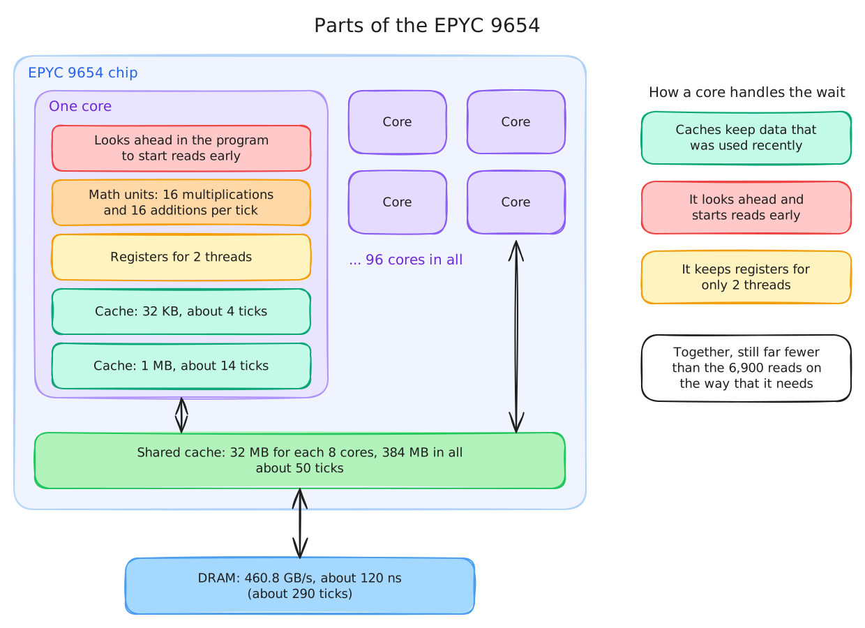
A chip does more operations per second when it has more math units. A math unit is small, so a chip can hold thousands of them. For example, the AMD EPYC 9654 is a server CPU from 2022 with 96 cores, where a core is one processor inside the CPU. Each core can do 16 multiplications and 16 additions on 32-bit numbers on every tick. At 2.4 GHz, the 96 cores together do about 7.4 trillion operations per second.
Memory bandwidth
Every number has to come from memory before a math unit can use it. The main memory is DRAM on separate chips next to the processor, and the numbers travel between the chips over wires. Each wire carries a limited number of bits per second, and there is room for only a limited number of wires at the edge of a chip.
The speed of reading memory is called the memory bandwidth, which is the number of bytes that the chip can read per second. The EPYC 9654 reads 460.8 GB per second, which is about 115 billion 32-bit numbers. In the same second, it can do about 7.4 trillion operations, which is 64 operations for each number that it reads. If a program does fewer than 64 operations on each number, the math units sit idle while they wait for the next numbers.
Most simple programs do much less than 64 operations per number. For example, y = a·x + y reads the two numbers x and y and does one multiplication and one addition. It does 1 operation per number, so the math units wait on memory for 63 of every 64 operations that they could do. A program with so little math per number is called memory bound, because the speed of memory sets its speed.
In the diagram, the two bars show the time to read the numbers and the time to do the math, for the same amount of work, on a chip that needs 64 operations per number. The longer bar sets the speed. You can change the number of operations that a program does on each number.
The gap grows with each new generation of chips, because designers can add math units faster than they can add bandwidth.
Memory latency
Each read also takes a long time to arrive. The time from asking for a number to getting it is called the latency, and on a real chip it is hundreds of ticks.
A read takes so long because of physics. At 2 GHz, one tick is half a nanosecond, and light moves only 15 cm in one tick. Electric signals in the wires of a chip move slower than light. The signals also pass through many stages of transistors on the way, and each stage takes one tick. A read has to go from the math unit to the memory and back through all of the stages.
On a server with the EPYC 9654, a read from main memory takes about 120 nanoseconds, which is about 290 ticks at 2.4 GHz. During one latency, the memory could deliver 460.8 GB per second times 120 nanoseconds, which is about 55,000 bytes. To use all of its bandwidth, the chip has to keep about 55,000 bytes of reads on the way at all times.
A program that works on one place of y = a·x + y at a time asks for 8 bytes, two 32-bit numbers, and then waits. The 8 bytes are 0.014% of 55,000 bytes, so the program uses 0.014% of the bandwidth. To use all of the bandwidth, the chip needs about 6,900 such reads on the way at the same time.
How a CPU handles latency
A CPU tries to make each wait shorter. It keeps caches, which are small, fast memories near the math units. A cache keeps recently used data, so a second read of the same data doesn’t have to go to the main memory.
A CPU also tries to ask for many numbers before it waits for the first one. The compiler, which is the program that turns code into instructions, rearranges the instructions to start reads early. The hardware also looks ahead in the program for reads that it can start, but it can track only a limited number of reads at a time, far fewer than 6,900.
A third way to get more reads on the way is to run many copies of the program at the same time, where each copy works on its own places in the lists. Each running copy of a program is called a thread. A thread has its own program counter and its own numbers to work on.
A thread keeps the numbers that it works on in registers, like r1 to r4 in the program above. A CPU core keeps the registers of only one or two threads. To run a different thread, the core must first save the registers of the old thread to memory and load the registers of the new one. Switching threads is slow on a CPU, so a CPU runs only one or two threads on each core.
A CPU is a latency machine, which means that it is built to finish each thread as fast as possible. Its cores spend much of their area on caches and on looking ahead in the program. Each core is large, so a CPU has at most about a hundred cores, and it can’t keep enough reads on the way for work like y = a·x + y.
A chip built for throughput
A chip for a very large amount of independent work can make the opposite choices. It needs the total work to finish fast, even if each thread is slow. The amount of work that a chip finishes per second is called throughput.
A throughput chip can follow two rules:
- Spend the chip area on math units and on space for many threads, and spend less on caches and on making one thread fast.
- Accept that each read waits a long time, and keep enough threads that some thread always has its numbers.
A GPU is a chip built with both rules. The rest of this note uses the NVIDIA H100 GPU as the example.
The H100 has 16,896 math units for 32-bit numbers, and NVIDIA calls them FP32 cores. Each one does a multiplication and an addition on every tick, and the chip runs at 1.98 billion ticks per second. The H100 does about 67 trillion operations per second, which is about 9 times the EPYC 9654.
The H100 also has much more bandwidth. Its memory is called HBM (high bandwidth memory), and it reads 3.35 TB per second, which is about 840 billion 32-bit numbers. The H100 needs 80 operations per number, close to the 64 of the EPYC 9654. 4 4. Designers keep the math and the bandwidth of a chip in about the same ratio, because extra math that always waits on memory is wasted area. The GPU has many times more of both, so programs that run at the speed of memory also run many times faster on it.
The latency of the H100 is longer than the CPU’s. A read from HBM takes about 650 ticks, which is about 370 nanoseconds. To use all of its bandwidth, the H100 needs 3.35 TB per second times 370 nanoseconds of reads on the way, which is about 1.2 MB. With 32-bit numbers, one place of y = a·x + y reads 8 bytes, so the H100 needs about 150,000 reads on the way at the same time.
Switching between threads
To keep 150,000 reads on the way, the chip needs more than 150,000 threads, and it must switch between them at no cost. A GPU therefore keeps the registers of every thread on the chip at all times. A part of the chip called the scheduler then picks, on each tick, one thread that isn’t waiting for data and runs its next instruction.
The diagram shows one scheduler and a few threads. Each thread runs a few math instructions and then starts a read, and it then waits 20 ticks for its data. A real read takes about 650 ticks, so a real chip needs many more threads than the diagram shows.
With a few threads, the scheduler has nothing to run on most ticks. With more threads, some thread is almost always ready, so the other threads run while one thread waits. More math between reads also helps, because each thread then has more work to do before it waits.
The H100 can keep 270,336 threads on the chip at the same time, which is more than the 150,000 that it needs. It has 33 MB of registers to hold their numbers. 5 5. A read needs a register to put its result in, so the registers also limit how many reads can be on the way. The H100’s 33 MB of registers can hold many times the 1.2 MB that its memory needs on the way. The registers are one more level of storage that hides the latency.
Warps
Before a thread can run an instruction, the chip has to fetch the instruction from memory and decode it, which means working out what the instruction asks for. Fetching and decoding take circuits and power. On a throughput chip, most threads run the same program on different numbers, so many threads need the same instruction at the same time.
The H100 therefore groups its threads in sets of 32, and each set is called a warp. The chip fetches and decodes one instruction for the whole warp, and all 32 threads run it at the same time, each on its own numbers. The scheduler picks a warp, not a single thread, on each tick.
6
6. The threads of a warp share one instruction, so they must also follow the same path through the program. When some threads of a warp take one side of an if and others take the other side, the warp runs both sides one after the other. The threads that didn’t take a side sit idle while that side runs.
The scheduler from the last diagram works the same way with warps. Each row is then a warp of 32 threads, and each instruction runs on 32 numbers at once.
SMs
One scheduler can’t feed a whole chip. The H100 is about 3 cm wide, and even light needs a fifth of a tick to cross 3 cm. Signals in the wires of a chip are slower than light, so a signal from a scheduler in the middle of the chip would use much of a tick, or more, only to reach the far math units and registers.
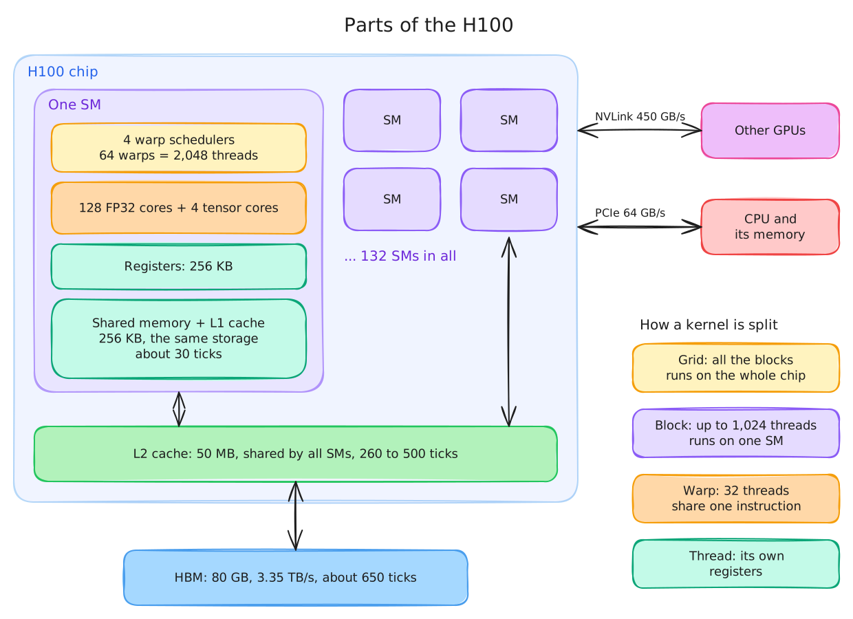
The H100 is therefore built from 132 copies of a smaller processor, and each copy is called an SM (streaming multiprocessor). Each SM has its own math units, registers and schedulers, so most signals only have to cross one SM.
| Part | One SM | Whole H100 |
|---|---|---|
| FP32 cores | 128 | 16,896 |
| Warp schedulers | 4 | 528 |
| Warps that it can keep | 64 | 8,448 |
| Threads that it can keep | 2,048 | 270,336 |
| Registers | 256 KB | 33 MB |
On each tick, each of the 4 schedulers of an SM picks one warp and runs one instruction for its 32 threads. The 4 schedulers together run 128 threads per tick, which matches the 128 FP32 cores. The SM keeps 64 warps, so on each tick at most 4 of them run, and the others wait for data or for their turn. 7 7. The 256 KB of registers on an SM are shared by all of its threads. With 2,048 threads, each thread gets 32 registers. A program that needs more registers per thread leaves room for fewer threads on the SM, so it has fewer threads to switch between while it waits for memory.
Blocks and shared memory
Some work needs threads to use each other’s results. For example, to add up a list of numbers, many threads can each add up one part of the list. Then the chip still has to add the partial sums together.
Threads on different SMs can share numbers only through HBM, which is slow. The H100 gives each SM a fast memory that its threads can share, called shared memory. Each SM has up to 228 KB of shared memory, and a read from it takes about 30 ticks instead of about 650.
A GPU program therefore puts its threads in groups called blocks. Each block has up to 1,024 threads, and all the threads of a block run on the same SM. The threads of a block can read and write the same shared memory. They can also wait for each other at a point in the program, so that every thread has finished writing before any thread reads.
A GPU program is called a kernel. When the CPU starts a kernel, it says how many blocks to run and how many threads each block has. All the blocks of one kernel together are called the grid.
| Level | Size | What it shares |
|---|---|---|
| Thread | 1 | Its own registers |
| Warp | 32 threads | One instruction at a time |
| Block | Up to 1,024 threads | One SM and its shared memory, and it can make its threads wait for each other |
| Grid | All the blocks of one kernel | Nothing, so the blocks run in any order |
For example, a kernel that brightens a picture of 1024 by 1024 pixels could use one thread for each pixel and blocks of 16 by 16 threads. The grid then has 4,096 blocks of 256 threads.
The blocks of a grid must not depend on each other, so the GPU can run them in any order on any SM. An SM can run several blocks at the same time, and it starts a new block when one finishes. The same kernel can run on a small GPU with a few SMs or on an H100 with 132. A grid with many more blocks than SMs keeps every SM busy.
The CPU and the GPU also work at the same time. When the CPU starts a kernel, it puts the kernel in a queue for the GPU and goes on to its next instruction. The CPU waits for the GPU only when it needs a result.
Levels of memory
A throughput chip still uses caches, because a read from a cache needs less bandwidth from HBM. Each SM of the H100 has an L1 cache, and all the SMs share one larger cache in the middle of the chip, which is called the L2 cache.
The L1 cache and shared memory are the same storage on the chip. Each SM has 256 KB of fast storage, and a kernel can set up to 228 KB of it as shared memory, while the rest works as the L1 cache. A kernel that uses more shared memory leaves less room for the L1 cache. The two parts differ in who decides what they keep:
- The hardware manages the L1 cache. When a thread reads a number from HBM, the hardware keeps a copy in the L1 cache, so that a second read of the same number is fast. The kernel can’t choose what stays in the L1 cache.
- The kernel manages shared memory. The kernel copies numbers into shared memory itself, and the numbers stay there until the kernel writes over them. All the threads of a block can read and write them.
The H100 also connects to other chips. NVLink is a direct link to other GPUs, and PCIe is the link to the CPU and its memory. A level of memory that is closer to the math units is smaller, but it has more bandwidth and a shorter latency.
| Level | Size | Bandwidth | Latency |
|---|---|---|---|
| Registers | 256 KB per SM, 33 MB in all | ||
| Shared memory and L1 cache | 256 KB per SM | About 33 TB/s | About 30 ticks |
| L2 cache | 50 MB | About 7 TB/s | About 260 to 500 ticks |
| HBM | 80 GB | 3.35 TB/s | About 650 ticks |
| Another GPU, over NVLink | 450 GB/s each way | ||
| CPU memory, over PCIe 5 | 64 GB/s each way |
A program that reads from a closer level needs less math per number to keep the math units busy. For the FP32 cores, a program needs 80 operations per number that it reads from HBM, 38 from the L2 cache and 8 from shared memory. Moving data between the GPU and CPU memory is slower still, so a program should keep its data on the GPU.
Reusing numbers
The amount of math per number depends on the problem, and for most problems it doesn’t grow when the problem gets bigger. In y = a·x + y, each number is used once, so a bigger problem has more numbers and the same 1 operation per number. A blur, which mixes each pixel of a picture with its neighbors, uses each number a fixed number of times, so its math per number is the same at any size.
Matrix multiplication is different, because each number is used many times. To multiply two matrices of size $n$ by $n$, the chip reads $2n^2$ numbers and does $2n^3$ operations, because each output is a sum of $n$ products. Each number is used $n$ times, which gives $n$ operations per number. A bigger matrix gives more math per number.
Neural networks are mostly matrix multiplications, so NVIDIA added math units that do only matrix multiplication, called tensor cores. A tensor core does a small matrix multiply in one step. With bf16 numbers, which is a 16-bit number format that takes 2 bytes, the H100’s tensor cores do 989 trillion operations per second.
8
8. Matrix multiplication is one of the few common problems with enough math per number to keep a GPU’s math units busy. Hardware for it can run at full speed, while faster hardware for y = a·x + y would only wait longer on memory.
The tensor cores need much more math per number than the FP32 cores. With bf16 numbers from HBM, they need about 590 operations per number, so a matrix multiply needs a size of about 590 to keep them busy. The gap also grows with each new generation of GPUs. From the V100 in 2017 to the H100 in 2022, the speed of the tensor cores grew about 8 times, from 125 to 989 trillion operations per second. In the same years, the bandwidth of HBM grew about 3.7 times, from 0.9 to 3.35 TB per second.
The diagram starts with tensor cores and a size of 256. You can change the problem, the math units and the level of memory that the numbers come from.
From shared memory, the tensor cores need only about 60 operations per number, so a size of about 60 is enough. A fast matrix multiply on a GPU therefore copies small pieces of the two matrices from HBM into shared memory, and then it uses each number there many times.
Overview
Further reading
- How GPU Computing Works (Jones, 2021)
- Making Deep Learning Go Brrrr From First Principles (He, 2022)
- Modal GPU Glossary
- How To Scale Your Model, the GPU chapter
- The Free Lunch Is Over (Sutter, 2005)
- AMD EPYC 9654 spec page
- AMD’s Zen 4 Part 1: Frontend and Execution Engine (Chips and Cheese, 2022)
- AMD’s Zen 4, Part 2: Memory Subsystem and Conclusion (Chips and Cheese, 2022)
- Testing AMD’s Bergamo: Zen 4c Spam (Chips and Cheese, 2023)
- NVIDIA H100 datasheet
- Dissecting the NVIDIA Hopper Architecture through Microbenchmarking and Multiple Level Analysis (Luo and others, 2025)